Vision and Mission of the Department
Vision
-
To be a center of excellence in Electronics Engineering with a specialization in VLSI Design and Technology, fostering innovation, research, and industry-ready education to empower students for global leadership in the field of semiconductor and electronics technology.
Mission
-
Inspire students to become leaders and entrepreneurs in the semiconductor and electronics industry by nurturing innovative thinking and management skills.
-
Equip students with hands-on experience in VLSI design, semiconductor tools, and cutting-edge technologies through advanced labs, projects, and industry internships.
-
Foster ethical values, technical expertise, and lifelong learning skills to prepare graduates for successful careers and leadership roles in the global electronics industry.
Program Educational Objectives(PEO's)
-
PEO1: Our Graduates will develop strong technical foundations in Electronics Engineering, with a specialization in VLSI Design and Technology, enabling them to analyze, design, and optimize semiconductor circuits and systems for real-world applications.
-
PEO2: Our Graduates will engage in research, innovation, and lifelong learning to adapt to evolving VLSI technologies, semiconductor advancements, and industry trends, contributing to technological growth and development.
-
PEO3: Our Graduates will exhibit leadership, teamwork, and ethical responsibility while addressing societal and industrial challenges through sustainable and efficient VLSI solutions, fostering entrepreneurship and professional excellence.
Program Specific Outcome (PSO's)
-
PSO1: Apply fundamental knowledge of electronics and advanced VLSI design techniques to model, analyze, and implement digital and analog systems using industry-standard tools and methodologies.
-
PSO2: Utilize modern EDA tools, FPGA platforms, and fabrication techniques to address real-world challenges in the semiconductor and electronics industry.
Programme Outcomes (PO's)
Students graduating from B.E. Electronics Engineering (VLSI Design and Technology) should be able to:
-
PO1: Engineering Knowledge: Apply knowledge of mathematics, natural science, computing, engineering fundamentals and an engineering specialization as specified in WK1 to WK4 respectively to develop to the solution of complex engineering problems.
-
PO2: Problem Analysis: Identify, formulate, review research literature and analyze complex engineering problems reaching substantiated conclusions with consideration for sustainable development. (WK1 to WK4)
-
PO3: Design/Development of Solutions: Design creative solutions for complex engineering problems and design/develop systems/components/processes to meet identified needs with consideration for the public health and safety, whole-life cost, net zero carbon, culture, society and environment as required. (WK5)
-
PO4: Conduct Investigations of Complex Problems: Conduct investigations of complex engineering problems using research-based knowledge including design of experiments, modelling, analysis & interpretation of data to provide valid conclusions. (WK8).
-
PO5: Engineering Tool Usage: Create, select and apply appropriate techniques, resources and modern engineering & IT tools, including prediction and modelling recognizing their limitations to solve complex engineering problems. (WK2 and WK6)
-
PO6: The Engineer and The World: Analyze and evaluate societal and environmental aspects while solving complex engineering problems for its impact on sustainability with reference to economy, health, safety, legal framework, culture and environment. (WK1, WK5, and WK7).
-
PO7: Ethics: Apply ethical principles and commit to professional ethics, human values, diversity and inclusion; adhere to national & international laws. (WK9)
-
PO8: Individual and Collaborative Team work: Function effectively as an individual, and as a member or leader in diverse/multi-disciplinary teams.
-
PO9: Communication: Communicate effectively and inclusively within the engineering community and society at large, such as being able to comprehend and write effective reports and design documentation, make effective presentations considering cultural, language, and learning differences.
-
PO10: Project Management and Finance: Apply knowledge and understanding of engineering management principles and economic decision-making and apply these to one’s own work, as a member and leader in a team, and to manage projects and in multidisciplinary environments.
-
PO11: Life-long Learning: Recognize the need for, and have the preparation and ability for i) independent and life-long learning ii) adaptability to new and emerging technologies and iii) critical thinking in the broadest context of technological change. (WK8)
Programme Highlights
The B.E. program in Electronics Engineering (VLSI Design and Technology) stands out for its dynamic curriculum and industry-relevant training. Key highlights of the program include:
1.Specialized Curriculum
-
Comprehensive coursework covering digital and analog VLSI design, semiconductor device fundamentals, low-power design techniques, and system-on-chip (SoC) architectures.
-
Inclusion of cutting-edge topics such as AI-based VLSI design, IoT hardware, and advanced fabrication technologies.
2.Industry-Relevant Training
-
Hands-on experience with industry-standard Electronic Design Automation (EDA) tools such as Cadence, Synopsys, and Mentor Graphics.
-
Emphasis on ASIC and FPGA design, verification methodologies, and design for testability (DFT).
3.State-of-the-Art Laboratories
-
Access to advanced VLSI and microelectronics labs equipped with the latest tools for circuit simulation, layout design, and hardware prototyping.
-
Facilities for semiconductor device characterization, PCB design, and embedded system development.
4.Collaborations with Industry
-
Strong ties with leading semiconductor companies and research organizations for internships, live projects, and industrial training.
-
Regular workshops, seminars, and guest lectures by industry experts to bridge the gap between academics and practical applications.
5.Research and Innovation Opportunities
-
Opportunities to work on real-world problems through capstone projects, research internships, and funded projects in VLSI and semiconductor technologies.
-
Encouragement to publish research in reputed journals and present at national and international conferences.
6.Experienced Faculty
-
Highly qualified faculty with expertise in VLSI design, embedded systems, and semiconductor technology, ensuring mentorship and guidance throughout the program.
7.Career-Focused Approach
-
Dedicated placement support with training in interview preparation, resume building, and technical skills enhancement.
-
Graduates are well-prepared for careers in semiconductor design, system integration, R&D, and emerging technologies like AI hardware and quantum computing.
This program is tailored to meet the demands of the fast-evolving electronics industry, providing students with the skills and knowledge required to thrive in VLSI design and technology roles.
Centre of Excellence
The Centre of Excellence (CoE) in VLSI Design and Technology serves as a hub for innovation, research, and skill development, supporting the B.E. program in Electronics Engineering (VLSI Design and Technology). This dedicated facility bridges the gap between academia and industry, fostering collaboration and preparing students to excel in the competitive semiconductor and electronics domain.
Key Features of the Centre
1.State-of-the-Art Infrastructure
-
Equipped with advanced Electronic Design Automation (EDA) tools from industry leaders such as Cadence, Synopsys, and Mentor Graphics.
-
Facilities for IC design, fabrication simulations, and testing, along with FPGA and ASIC prototyping capabilities.
2.Industry Partnerships
-
Collaborative initiatives with leading semiconductor companies, enabling access to the latest technologies and methodologies.
-
Memorandums of Understanding (MoUs) with global technology giants for live projects, internships, and skill enhancement.
3.Research and Innovation
-
Focused on cutting-edge research areas such as low-power VLSI design, SoC architectures, 3D ICs, and AI-driven chip design.
-
Encourages student participation in research projects, enabling them to publish in prestigious journals and present at conferences.
4.Skill Development and Training
-
Regular workshops, certification programs, and hands-on training sessions to develop industry-ready skills.
-
Emphasis on real-world problem-solving through project-based learning and design challenges.
5.Incubation and Entrepreneurship Support
-
Supports student-driven startups and entrepreneurial ventures in VLSI and semiconductor technology.
-
Provides mentorship, funding opportunities, and guidance for transforming innovative ideas into viable solutions.
6.Expert Mentorship
-
Guidance from experienced faculty, industry professionals, and researchers in specialized fields of VLSI design and technology.
-
Regular interaction with alumni and industry leaders to inspire innovation and career growth.
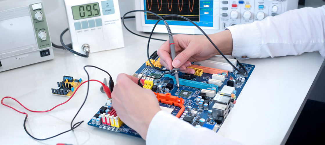
Department Lab Facilities
The Department of Electronics Engineering offers world-class laboratory facilities to support the B.E. program in VLSI Design and Technology. These specialized labs provide students with hands-on experience in designing, testing, and implementing advanced electronics and VLSI systems.
Key Lab Facilities
1.VLSI Design Laboratory
-
Equipped with industry-standard Electronic Design Automation (EDA) tools such as Cadence, Synopsys, and Mentor Graphics.
-
Workstations for digital and analog IC design, verification, and simulation.
-
Facilities for RTL design, synthesis, and physical layout generation.
2.FPGA and Embedded Systems Lab
-
Access to high-performance FPGA development boards such as Xilinx and Altera for real-time prototyping.
-
Support for programming and testing of embedded systems using ARM, PIC, and AVR microcontrollers.
-
Integration of hardware and software solutions for IoT and automation applications.
3.Digital and Analog Electronics Lab
-
Comprehensive setups for designing, testing, and troubleshooting digital and analog circuits.
-
Oscilloscopes, logic analyzers, and signal generators for circuit analysis and debugging.
-
Focus on practical learning through implementation of amplifiers, filters, oscillators, and signal processing circuits.
4.ASIC Design and Testing Lab
-
Facilities for ASIC design flow, including design entry, synthesis, floor planning, placement, routing, and verification.
-
Tools for power and timing analysis, ensuring designs meet performance and reliability standards.
5.Advanced Simulation Lab
-
Software for system-level simulation, including Cadence Design Tools, Ansys Semiconductor Tools, Xilinx ISE Tool, MATLAB/Simulink, SPICE, and Multisim.
-
Hands-on experience in modeling and analyzing complex systems, including SoCs and mixed-signal designs.
6.High-Performance Computing Lab
-
Advanced computing systems for handling large-scale simulations and computational tasks related to VLSI and embedded systems.
-
Parallel processing systems and cloud-based EDA tools for efficient design workflows.
Laboratory Highlights
-
Regular updates with the latest tools and equipment to stay aligned with industry advancements.
-
Emphasis on practical training and project-based learning for enhanced skill development.
-
Support for student projects, research activities, and innovation challenges.
-
Guidance from experienced lab instructors and faculty to ensure students gain industry-ready expertise.
The department's lab facilities play a crucial role in providing students with the technical knowledge and hands-on skills needed to excel in the field of VLSI design and technology.
Student Activities
The B.E. program in Electronics Engineering (VLSI Design and Technology) encourages students to engage in a wide range of activities beyond academics, fostering their technical, creative, and leadership skills. These activities enhance learning, promote teamwork, and prepare students for dynamic careers in the field of electronics and VLSI design.
Technical Activities
1.Workshops and Seminars
-
Hands-on workshops on VLSI design tools, FPGA programming, and circuit prototyping.
-
Expert lectures and seminars on topics like semiconductor trends, AI in VLSI, IoT hardware, and low-power design.
2.Hackathons and Competitions
-
Participation in national and international hackathons, coding challenges, and design competitions.
-
Opportunities to solve real-world industry problems in areas such as chip design, system-on-chip (SoC) integration, and embedded systems.
3.Research and Innovation Projects
-
Encouragement to undertake research projects under faculty mentorship, contributing to advancements in VLSI and semiconductor technology.
-
Presentation of innovative ideas at conferences, symposiums, and project exhibitions.
4.Industrial Visits and Internships
-
Regular visits to semiconductor manufacturing units, R&D centers, and design labs to gain practical insights into industry processes.
-
Internships with leading companies to gain hands-on experience in VLSI design, verification, and fabrication.
5.Technical Clubs and Committees
-
Active participation in department-run clubs focused on electronics, VLSI, and embedded systems.
-
Opportunities to lead and organize events such as technical quizzes, design challenges, and circuit debugging contests.
Co-Curricular and Extracurricular Activities
1.Tech Fest and Exhibitions
-
Organization and participation in annual technology festivals showcasing innovative projects and prototypes.
-
Collaboration with peers to design and present solutions to pressing technological challenges.
2.Leadership and Entrepreneurship Initiatives
-
Involvement in entrepreneurship cells to develop business ideas related to VLSI and electronics.
-
Participation in leadership programs and soft skills workshops to enhance professional growth.
3.Community Outreach
-
Conducting technical workshops and awareness programs for schools and local communities.
-
Volunteering in social initiatives that use electronics and technology for societal benefit.
4.Cultural and Sports Events
-
Active involvement in cultural events, music, dance, and dramatics for holistic development.
-
Participation in interdepartmental and intercollegiate sports competitions to promote teamwork and fitness.
Highlights of Student Activities
-
A balanced blend of technical and extracurricular engagements to develop well-rounded professionals.
-
Regular mentorship from faculty and industry experts to guide students in their academic and professional pursuits.
-
Opportunities to showcase talent, build networks, and create a strong foundation for future career growth.
These activities aim to nurture creativity, innovation, and leadership among students while fostering a vibrant and engaging learning environment.
Regulation, Curriculum & Syllabi
Regulation
Curriculum & Syllabi